| ||||||||
 | ||||||||
Electrodeposition Electrodeposition may be considered one of the most adaptable and cost effective methods for the large scale deposition of elemental and compound semiconductors. These films may find application in photovoltaic and display devices.
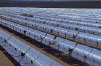
Picture above is a typical solar energy farm |
Photovoltaics Introduction: Photovoltaic solar cells are composed of various semiconductor materials such as single crystal, polycrystalline or amorphous Silicon, Cadmium Telluride, Copper Indium Diselenide (CIS), Copper Indium Gallium Diselenide (CIGS), Gallium Arsenide and Indium Phosphide. More recently organic semiconductors and dye sensitized solar cells have also received attention. One of the most cost effective (and in our estimation, one of the most under utilized) methods of producing the semiconductor layers is electrodeposition. Electrodeposition - The Background: The main barrier to photovoltaic cells penetrating the mass market is the prohibitive cost of the solar panels. More cost effective method of manufacture are constantly being sought. Electrodeposition may be considered to be one of the least expensive and most flexible approaches for the large scale deposition of solar grade semiconductors. For example, the successful electrodeposition of the II-VI semiconductor CdTe has been successfully achieved and this approach has been the basis for the commercial production of thin film CdS/CdTe photovoltaic cells. Electrodeposition of II-VI Semiconductors: There are numerous examples of II-VI semiconductors that are amenable to electrodeposition. Typical examples include CdTe, CdSe, CdS, CdHgTe, ZnS, CIS and CIGS etc. Successful electrodeposition may be achieved using aqueous, non-aqueous and molten salt electrolytes. Perhaps the best studied is CdTe in which very high purity thin films have been deposited from acidic solutions of Cd2+ and HTeO2+. The fundamental processes for allowing the CdTe deposition have been patented by Jerry Barker and co-workers. These processes have been exploited by BP Solar as the basis of the Apollo thin film CdTe photovoltaics project in Fairfield, California. This project successfully deposited substrates up to 1 m2. The recent success of First Solar's CdS/CdTe technology has clearly illustrated the commercial viability of this thin film PV. Other companies such as PrimeStar Solar are also attempting to enter the market with CdS/CdTe cells. Clearly, in our view the electrodeposition of CdTe is a commercial success waiting to happen. Electrodeposition of III-V Semiconductors: Example materials that have been successfully electrodeposited include GaAs, InP and GaP. PV devices made from these materials often have high conversion efficiencies, so the motivation to develop low cost methods of deposition is compelling. To date, in almost all cases, the electrodeposition process has been carried out in molten salt electrolytes, and careful control of the bath conditions is required to allow high purity deposits. In addition, this approach generally increases the material costs due to the relative complexity of the deposition equipment. Clearly, new directions are required and further work on non-aqueous systems may well yield improved performance and costs. Electrodeposition of Elemental Semiconductors: Si and Ge have both been successfully electrodeposited using molten salt and non-aqueous electrolytes. The deposition of these elements is thermodynamically favored so additional work in this area may well yield improved results, offering the possibility of low-cost PV grade materials. Some of the key problems to overcome will be related to deposit purity, morphology and surface reactivity. Additional work on bath precursors will also be necessary. New Directions: Electrodeposition may be employed for the successful deposition of a range of semiconductors. By careful selection of deposition equipment, electrolyte, temperature, precursors, deposition conditions, doping levels and control of the impurity content, it is thermodynamically possible to deposit high purity films of Si, CdTe, GaAs, InP, CIS and many others. We offer the capability to design and construct plating systems to allow for the large area commercial deposition of these technologically important materials.
|

| Copyright© 2002-2010
Jerry Barker Consultants Limited. Registered in England and Wales, Company No: 7095860 |